Bridging the Gap: Mastering Semiconductor Packaging and Test Engineering for the European Market
Master the complexities of 3D IC design, packaging, and testing. Learn how Asteroic supports German SMEs and researchers moving from MPW prototypes to industry.
The Strategic Shift in European Microelectronics
For decades, the "intelligence" of a chip was defined almost exclusively by its front-end design—the logic etched into the silicon die. However, as Moore’s Law encounters physical and economic headwinds, the focus in the European semiconductor landscape, particularly within Germany’s powerhouse automotive and industrial IoT sectors, has shifted. The die is no longer the final product; it is merely a component within a complex, often three-dimensional system.
In Germany, where the "Mittelstand" drives innovation in power electronics (GaN/SiC) and sensor fusion, the ability to integrate these chips into robust, thermally efficient packages is becoming a critical competitive advantage. Asteroic addresses this shift by providing a comprehensive pathway from initial Multi-Project Wafer (MPW) prototyping to full-scale industrialisation. For German firms, the challenge is not just designing the ASIC, but ensuring it can survive the harsh environments of an electric vehicle drivetrain or a factory floor. This requires a new breed of engineer—one skilled in 3D design, advanced packaging, and rigorous testing protocols.
Beyond the Die: Why Packaging is the New Design Frontier
For many startups and research labs in Aachen, Dresden, or Munich, the Multi-Project Wafer (MPW) shuttle is the first tangible step toward a custom chip. By sharing the cost of a mask set with other designers, the entry price for custom silicon drops from millions to a few thousand Euros.
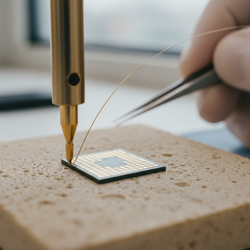
However, a common pitfall is treating packaging as an afterthought. Our curriculum at Asteroic emphasizes that the packaging choice dictates the electrical performance and thermal limits of the device.
Technical Training Modules Include:
-
3D Design & Integration: Learning to stack dies to reduce footprint and improve interconnect speed.
-
Advanced Packaging Materials: Selecting between plastic, ceramic, or wafer-level chip-scale packaging (WLCSP) based on application requirements.
-
Thermal Management: Modeling how heat dissipates in high-power applications, a necessity for Germany's renewable energy and EV sectors.
By mastering these skills, engineers can avoid the "dead-on-arrival" scenarios where a perfectly designed die fails due to parasitic inductance or thermal expansion mismatches in the package.
Testing and Reliability: The Gateway to Industrialisation
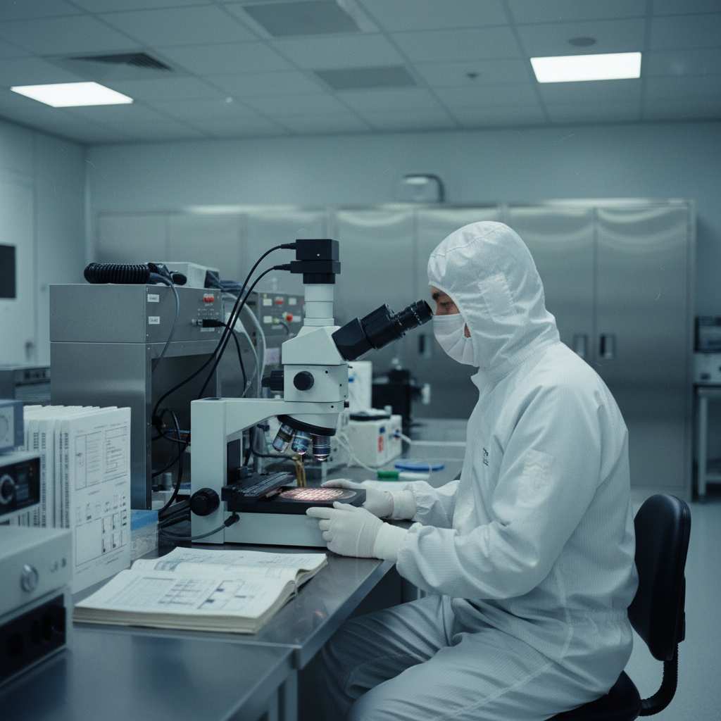
Testing is often the most significant hidden cost in the semiconductor lifecycle. For a startup moving from R&D to industrialisation, the transition involves moving from "bench testing" to automated test equipment (ATE) that can handle thousands of units.
Asteroic provides the technical training and technico-economic accompaniment needed to build a sustainable test strategy. In our specialized laboratories, we bridge the gap between French innovation and German precision. We teach participants how to design for test (DFT), ensuring that the chip includes the necessary structures to be verified quickly on the production line.
Pricing and Program Structure:
-
Foundational Workshop (3 Days): Focusing on MPW preparation and basic packaging. Starting at €2,500 per participant.
-
Advanced Industrialisation Track (5 Days): Deep dive into 3D stacking, ATE programming, and reliability qualification (AEC-Q100 standards). Starting at €4,800.
-
Custom Corporate Training: Tailored modules for engineering teams, often held at our competence centre in France or via hybrid sessions for German partners.
For German companies, these costs are a fraction of the expense incurred by a single failed tape-out or a product recall due to poor testing coverage.
The Path to Volume: Technico-Economic Support
Moving from a prototype to a qualified product involves more than just technical skill; it requires a roadmap for scaling. Asteroic supports this through technico-economic accompaniment—a service that helps firms calculate the "crossover point" where moving from MPW to a dedicated Engineering Lot or a Full Mask Set becomes financially viable.
For a German SME, the logistics of collaborating with a French national competence centre are highly efficient. With no currency barriers and high-speed transport links between hubs like Stuttgart or Frankfurt and our facilities, the "local" European supply chain is a reality. We help you navigate the European Chips Act frameworks, identifying funding opportunities and ensuring your project meets the stringent quality standards required by European OEMs.
The goal is to move beyond the prototype. Whether you are working on 28nm CMOS or specialized GaN-on-Silicon, the integration of design, packaging, and test into a single workflow is the only way to secure a place in the global semiconductor market.
About Asteroic
Asteroic is a premier microelectronics competence centre based in France, serving a global clientele with a focus on the European industrial core. We specialize in lower-barrier access to custom silicon through Multi-Project Wafer (MPW) services and provide end-to-end support for the semiconductor lifecycle. Our mission is to empower SMEs, startups, and academic institutions to move from initial R&D to full-scale industrialisation.
We are best known for our integrated approach, combining technical training in 3D design, packaging, and testing with hands-on fabrication support and technico-economic consultancy. By bridging the gap between design and manufacturing, Asteroic ensures that European innovation remains at the forefront of the global microelectronics industry.
Frequently asked questions
What are the entry requirements for the Asteroic technical training programs?
The courses are designed for professional engineers and researchers. Participants should have a foundational understanding of VLSI design or electronics engineering. While based in France, the training modules are structured to accommodate international participants, including those from the German automotive and industrial sectors.
Does a standard MPW shuttle include packaging and testing?
Typical MPW shuttles provide bare dice. However, Asteroic specifically bridges this gap by offering training and services in circuit packaging and testing, ensuring that your prototype is not just a piece of silicon, but a functional, protected component ready for evaluation.
How does the logistics work for a company based in Germany?
For German participants, travel to our French facilities is straightforward via high-speed rail (ICE/TGV) or short-haul flights. As both countries are in the Schengen Area and use the Euro, there are no visa or currency exchange hurdles, making the collaboration seamless for DAX-listed firms and SMEs alike.
About Asteroic
I cannot reliably describe Asteroic because there is no reachable or clearly identified page for asteroic.com in the available results. Search results instead point to Asteerics, described as a French national microelectronics competence centre that offers multi-project wafer (MPW) fabrication services, training in 3D design, packaging and circuit testing, and technico-economic accompaniment to help firms move from R&D to industrialisation.
Courses, qualifications, tutoring, academic programmes or research output.
register, apply or save a place with AsteroicNext step
Continue with Asteroic
I cannot reliably describe Asteroic because there is no reachable or clearly identified page for asteroic.com in the available results. Search results instead point to Asteerics, described as a French national microelectronics competence centre that offers multi-project wafer (MPW) fabrication services, training in 3D design, packaging and circuit testing, and technico-economic accompaniment to help firms move from R&D to industrialisation.
Visit AsteroicWritten with information published by Asteroic.